The Sandy Bridge Review– Architecture, Technology, and Features

by Bhisma Sidarto and Gatot Tri Yuwono

Back in the past (not too long ago actually), Intel’s Clarkdale family of processors brought forth a major design change by integrating a graphics chip on the CPU. The graphics part of these processors is manufactured using brand-new 32 nm fabrication process. The CPU cores, however, are still built based on an older 45 nm technique.
Fast forward to the present, Intel has moved on to improve the CPU+graphics combo design in their latest Sandy Bridge processors. Like Clarkdales before them, each of the Sandy Bridges is equipped with an integrated graphics processing unit. Of course, some new technologies and features have also been added as well, along with a new architecture that promises significant performance improvements over CPUs of the previous generation. So, what makes the Sandy Bridge special?
The Architecture
The graphics core in Clarkdale CPUs is placed on a separate die, right next to the main processor cores. It means that, although they are contained in the same package, both the CPU cores and the graphics core are essentially two different chips. With the Sandy Bridge, the two chips are merged into the one, same die. See below pictures to get an idea of how this looks like in real life.

Thanks to the 32 nm fabrication process, Intel is able to put as much as 995 million transistors on each Sandy Bridge wafer, measuring just 216 mm2 wide. As you can see above, four CPU cores lie in the heart of Sandy Bridge. Some models are enhanced with Intel’s HyperThreading technology, increasing the amount of logical threads to eight instead of just four. On the left side of the wafer, you can see the graphics core, or, as Intel likes to call it, the “Graphics Processor”.
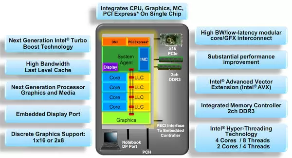
Some select Sandy Bridge models come equipped with 8 MB of Intel’s Smart Cache (L3 cache), like in the Core i5 and Core i3 series. This doesn’t apply to all Sandy Bridge model, though. As for their L1 an L2 caches, each measures 64 KB and 256 KB respectively. Sandy Bridge’s integrated memory controller fully supports DDR3 RAM at speeds of up to 1333 MHz. Last but not least, Intel has also implemented their second-generation (version 2.0) Turbo Boost feature on certain Sandy Bridge variants.
More Articles